-
- Contact Us
- Privacy Policy
- term and condition
- Cookies policy
APT50GH120BSC20 Power Module: Latest Performance Report
Point: The APT50GH120BSC20 is presented by the manufacturer as a 1200 V, 50 A Fast Field‑Stop IGBT paired with an integrated SiC diode in a TO‑247 package; this report consolidates datasheet curves, lab benchmarking approaches, and practical design guidance to evaluate real‑world performance. Evidence: Microchip’s published datasheet provides the core VCE, switching energy, thermal impedance and SOA curves used throughout this analysis. Explanation: The goal is to give power electronics engineers, design leads, and procurement teams a concise, data driven assessment of whether the APT50GH120BSC20 meets modern high‑power switching needs and what to test first. Link: Refer to the Microchip datasheet for raw curves and recommended limits for further validation.
Point: This report covers device background, electrical and thermal performance, recommended test methodology, integration practices, and market positioning to enable rapid evaluation. Evidence: Sections mirror standard qualification flows used in bench characterization and system integration. Explanation: Readers will gain actionable KPIs (Eon/Eoff, conduction loss, Zth), step‑by‑step test setups, and a short checklist for selection or prototype procurement. Link: Use the datasheet figures as the baseline for comparisons and for parameter extraction.
1 — Background & Device Overview (Background)
1.1 Device specifications summary
Point: Key electrical and mechanical specifications define the integration envelope for the APT50GH120BSC20. Evidence: Manufacturer datasheet lists the following nominal values and limits. Explanation: The table below summarizes the primary specs engineers use during initial selection and thermal budgeting. Link: All values are consistent with the Microchip datasheet and should be cross‑checked against the actual lot release data.
| Parameter | Value / Note |
|---|---|
| Voltage rating | 1200 V (blocking) |
| Current rating | 50 A (continuous, case temp limited) |
| Package | TO‑247 |
| Topology | Fast Field‑Stop IGBT + integrated SiC diode |
| Max junction temperature | Typically 150 °C (see datasheet limit) |
1.2 Architecture & key features
Point: The field‑stop IGBT structure reduces tail charge and improves turn‑off speed versus conventional IGBTs, and the integrated SiC diode reduces reverse recovery losses. Evidence: Datasheet switching curves show reduced Eoff and improved dV/dt tolerance compared to legacy designs. Explanation: In practice, the field‑stop doping profile shortens minority‑carrier lifetime during turn‑off leading to lower switching energy, while the SiC diode’s limited recovery current reduces diode‑related switching spikes; together these traits improve converter efficiency at medium‑to‑high frequencies. Link: Confirm specific Eon/Eoff tradeoffs on the datasheet switching energy plots when defining gate drive and snubber strategy.
1.3 Typical applications & target markets
Point: The device targets traction inverters, solar and battery inverters, motor drives and UPS systems where 1200 V blocking and 50 A capability are typical. Evidence: Application notes and datasheet suggested use cases highlight traction and industrial drives. Explanation: For traction and high‑power motor drives the device’s reduced switching losses and robust diode recovery are advantageous at switching frequencies in the single‑ to low‑tens of kHz range; for solar inverters the thermal and SOA margins dictate cooling designs. Link: Use the datasheet’s thermal and SOA charts to match application duty cycles and switching frequency requirements.
2 — Electrical Performance Analysis (Data)
2.1 Switching characteristics (turn‑on/turn‑off)
Point: Important switching metrics to measure are rise/fall times (tr, tf), turn‑on/turn‑off delay (tq), dV/dt, gate charge and energy per event (Eon, Eoff)—these determine converter switching loss per kHz. Evidence: Datasheet switching energy curves provide Eon/Eoff vs. Ic and VCE conditions which are the reference for lab verification. Explanation: In bench tests, expect datasheet Eon/Eoff to be a best‑case measured at specific gate resistances and inductance; parasitic inductance, gate drive impedance, and measurement clamp networks will typically increase measured energy by 10–30%. Suggested figure: capture switching waveforms (VCE, IC, VGE) with ≥200 MHz oscilloscope bandwidth and appropriately rated current probes to resolve di/dt and dV/dt transients. Link: Use the datasheet switching waveform conditions to reproduce comparable bench setups.
2.2 Conduction behavior & losses
Point: Conduction loss is dominated by VCE(sat) across Ic and temperature; quantify Pcond = VCE(sat) × Ic averaged over the conduction interval. Evidence: Manufacturer VCE vs Ic curves and temperature coefficients show VCE rise with junction temperature. Explanation: Example calculation — assuming VCE(sat) = 1.2 V at 25 °C and 1.6 V at 125 °C at Ic = 50 A: Pcond@25 °C = 1.2 V × 50 A = 60 W; Pcond@125 °C = 1.6 V × 50 A = 80 W. This 33% increase highlights the impact of thermal derating on steady losses and the importance of keeping junction temperature low. Link: Cross‑reference the datasheet conduction curves and temperature coefficients when modeling inverter losses.
2.3 Dynamic behavior under transient loads
Point: Short‑circuit withstand, unclamped inductive switching behavior and SOA margins determine robustness under faults and transients. Evidence: Datasheet provides transient thermal impedance Zth(j‑c) vs time and SOA boundaries for pulsed conditions. Explanation: Use Zth(j‑c) to convert pulse energy into delta‑Tj for short pulses (e.g., 100 µs–10 ms); likewise, ensure unclamped inductive switching events do not exceed the instantaneous SOA or the diode avalanche limits. Practical bench validation should include single‑pulse and repetitive pulse sequences to map real thermal response against datasheet curves. Link: Validate with the datasheet’s transient Zth plots and SOA diagrams before qualifying a design for field deployment.
3 — Thermal Performance & Reliability (Data)
3.1 Thermal impedance and cooling requirements
Point: Thermal design requires understanding both steady‑state Rth(j‑c)/Rth(c‑a) and transient Zth for pulsed loads. Evidence: Datasheet lists junction‑to‑case Rth and Zth(j‑c) vs pulse duration. Explanation: For continuous operation, compute required heatsink thermal resistance: Rth_required = (Tj_max − Tamb − P×Rth_case‑sink)/(P), where P is total dissipated power. For example, a 60 W steady loss and 100 °C max junction yields a required overall thermal path to limit ambient rise; forced convection or a dedicated heatsink plate is typically necessary for 50 A continuous use in TO‑247. Link: Use the datasheet Rth and Zth curves to size heatsinks and cooling fans for your duty cycle.
3.2 Lifetime & derating guidelines
Point: Continuous operation near Tmax accelerates wear mechanisms; conservative derating extends lifetime. Evidence: Datasheet recommended maximum junction temperatures and derating notes provide acceptable operating envelopes. Explanation: Practical derating: for continuous operation target
3.3 Failure modes & reliability testing to prioritize
Point: Typical failure modes include bond lift, gate oxide breakdown, and diode avalanche or thermal runaway; prioritize tests accordingly. Evidence: Industry reliability data for field‑stop IGBTs and SiC diodes show prevalence of bond wire fatigue under thermal cycling and oxide degradation under repetitive VGE stress. Explanation: Recommended tests: power cycling (to stress bond wires and solder interfaces), thermal shock, gate overstress, and avalanche/short‑circuit endurance; include statistical sampling to establish mean cycles to failure. Link: Correlate failure signatures from testing against datasheet SOA and transient limits to refine system protections.
4 — Benchmarking & Test Methodology (Method)
4.1 Recommended test setups & measurement points
Point: Standardized switching test schematics improve repeatability and traceability when comparing devices. Evidence: Typical switching bench uses a clamp diode, inductive load, VDC source, gate driver with adjustable Rg, and measurement nodes at VCE, IC and VGE. Explanation: Critical measurement specs: oscilloscope ≥200 MHz (preferably 500 MHz for sharp edges), current probe bandwidth matching di/dt, and low‑inductance measurement leads. Place voltage probes close to the device terminals and minimize loop inductance to avoid measurement artifacts. Link: Reproduce the datasheet’s test conditions (Vdc, gate drive, Lload) to validate your bench against published curves.
4.2 Repeatable procedures for electrical & thermal tests
Point: Define step‑by‑step procedures and environmental controls to ensure comparable results. Evidence: Repeatability improves when ambient temperature and drive conditions are tightly controlled and when sample size is sufficient. Explanation: Procedure highlights: stabilize ambient at 25 ±2 °C for electrical tests, use a minimum of 5 samples for statistical confidence, document Vdc, Ic, switching frequency and gate resistor. For thermal tests, allow steady‑state to settle and log junction (or case) temperatures with calibrated sensors. Link: Standardize reporting format to include raw waveform captures, test conditions, and sample statistics.
4.3 Data analysis templates & KPIs
Point: Key KPIs to extract are Eon, Eoff, Qg, total switching loss per kHz, conduction loss at defined temperatures, thermal rise per watt, and SOA margin. Evidence: Plotting Eon/Eoff vs Ic and loss vs switching frequency provides immediate comparisons across devices. Explanation: Recommended outputs: switching energy tables, loss vs current charts, normalized efficiency vs frequency curves, and a thermal map for typical duty cycles. These deliverables enable rapid tradeoff decisions for BOM and cooling design. Link: Use the datasheet curves as a reference baseline when filling templates.
5 — Design Integration & Practical Recommendations (Method/Action)
5.1 Gate drive and protection recommendations
Point: Proper gate drive selection and active protection are critical for achieving the datasheet performance in system contexts. Evidence: Datasheet gate charge and recommended VGE limits set the acceptable drive window. Explanation: Suggested practices: pick gate resistance to balance dv/dt and switching loss (start with Rg ~5–10 Ω for bench tuning), implement Miller clamp or active turn‑off to prevent spurious turn‑on, and include desaturation detection with timed shutdown for short‑circuit protection. Ensure gate drive isolation and common‑mode transient immunity are specified for your system voltage environment. Link: Verify drive levels against the datasheet’s recommended VGE(max/min) and charge curves.
5.2 PCB layout, package mounting & cooling best practices
Point: Mechanical mounting, thermal interface materials (TIM), and PCB copper influence thermal performance significantly for TO‑247 parts. Evidence: Thermal contact resistance and clamping torque directly affect junction‑to‑case and case‑to‑heatsink conduction. Explanation: Best practices: use recommended torque for mounting screws, thin but thermally conductive TIM to minimize interface resistance, large copper pour on the case underside if applicable, and thermal vias to spread heat on multi‑layer boards. For high duty cycles, prefer direct clamping to a heatsink plate and forced convection. Link: Cross‑check mounting torque and TIM specs with the manufacturer’s assembly notes in the datasheet.
5.3 System‑level protections & EMI/ snubber strategies
Point: Snubber topology and EMI mitigation will affect both performance and regulatory compliance. Evidence: Datasheet switching transients indicate expected dV/dt and di/dt ranges which inform snubber selection. Explanation: For high switching speed, RCD snubbers limit voltage spikes and clamp energy with modest power dissipation; RC snubbers reduce dv/dt but incur continuous losses. Use common‑mode chokes, proper decoupling bank placement near DC link, and minimize loop area to reduce radiated EMI. Balance snubber losses against switching loss improvements to find the optimal tradeoff. Link: Use datasheet transient figures to size snubber components conservatively.
6 — Comparative Case Study & Market Positioning (Case)
6.1 Head‑to‑head comparison vs comparable 1200 V / 50 A devices
Point: Engineers must compare switching loss, conduction loss, thermal impedance, package and supply chain factors across vendors. Evidence: Benchmarked KPIs (Eoff, VCE(sat), Rth) are primary differentiators in similar packages. Explanation: A concise comparative table (below) should include the APT50GH120BSC20 alongside two comparable devices from major vendors, listing Eon/Eoff at a representative Ic, VCE(sat) at 25/125 °C, and Rth(j‑c). This allows quick prioritization based on system‑level efficiency or thermal constraints. Link: Use datasheet numbers as a baseline and validate with bench measurements before final selection.
| Device | Eoff @ 50 A (mJ) | VCE(sat) @50 A (V) | Rth(j‑c) (°C/W) |
|---|---|---|---|
| APT50GH120BSC20 | Refer to datasheet curve | Refer to datasheet curve | Refer to datasheet |
| Competitor A (1200 V / 50 A) | Bench value needed | Bench value needed | Bench value needed |
| Competitor B (1200 V / 50 A) | Bench value needed | Bench value needed | Bench value needed |
6.2 Cost vs performance tradeoffs and BOM impact
Point: Device selection impacts system efficiency, cooling requirements and overall BOM cost. Evidence: Higher performing parts can reduce heatsink size or fan power, offsetting higher unit cost over system lifetime. Explanation: Example TCO scenario: a 1% system efficiency improvement at full load for a 10 kW motor drive can translate to significant annual energy savings; weigh that against incremental device cost and any additional required board space or snubbing components. Early prototyping should quantify these tradeoffs with measured loss curves. Link: Use the benchmarking KPIs to populate a BOM impact model for your product.
6.3 Selection checklist for engineers
Point: A short checklist accelerates go/no‑go decisions for prototypes and procurement. Evidence: Practical factors include voltage/current margins, switching frequency, thermal budget, SOA needs, and supply risk. Explanation: Recommend using a checklist that captures required Vdc margin, peak and RMS currents, expected switching frequency, cooling capacity, lifetime targets, and acceptable unit cost. If the design demands moderate switching frequency (≤20 kHz) with a focus on reduced diode recovery loss, the device’s Fast Field‑Stop IGBT plus SiC diode is a strong candidate. Link: Validate checklist entries against datasheet limits and bench test results.
Conclusion
Point: The APT50GH120BSC20 demonstrates attributes—Fast Field‑Stop switching and an integrated SiC diode—that make it a compelling Power Module option for many medium‑power converters seeking improved efficiency and reduced diode recovery losses. Evidence: Datasheet switching and thermal curves indicate competitive Eon/Eoff and thermal impedance characteristics, with recommended limits for continuous and pulsed operation. Explanation: For engineers designing traction inverters, motor drives or inverters where switching Performance and thermal management are primary concerns, this part is worth prototype evaluation; primary caveats are the need for careful thermal design and conservative derating for continuous 50 A operation. Link: Begin with the benchmark procedures and thermal checks recommended above and confirm with the Microchip datasheet during prototype testing.
Key Summary
- Fast Field‑Stop IGBT plus integrated SiC diode offers reduced switching and recovery losses, improving converter efficiency when switching Performance matters; validate with Eon/Eoff bench tests.
- Thermal design is critical: conduction losses increase significantly with temperature—expect ~30% higher conduction loss at high junction temperature for typical VCE(sat) shifts.
- Benchmark using standardized test setups (defined Vdc, Rg, Lload) and extract KPIs (Eon/Eoff, Qg, Rth/Zth, SOA margin) to inform BOM and cooling tradeoffs.
- Gate drive, snubber and PCB layout decisions materially affect measured Performance—optimize Rg, minimize loop inductance, and apply appropriate snubber topology.
- Use the datasheet as the baseline for initial selection, then confirm with sample‑level testing for production readiness and reliability assurance.
Frequently Asked Questions
What are the key switching loss characteristics of the APT50GH120BSC20?
The APT50GH120BSC20’s switching loss characteristics are defined by datasheet Eon and Eoff curves which should be reproduced on the bench using the same Vdc, gate drive, and load inductance conditions. Practical measurements often show 10–30% higher energy due to parasitics; therefore, engineers should capture switching waveforms with high‑bandwidth probes and account for board inductance when estimating converter switching Performance.
How should engineers size cooling for continuous 50 A operation of the APT50GH120BSC20?
Cooling sizing begins with total dissipated power (conduction + switching). Use the datasheet Rth(j‑c) and Zth for pulse behavior to compute allowable thermal path; for 50 A continuous example, anticipate steady conduction losses on the order of tens of watts and size heatsink/fan to keep Tj below conservative limits (e.g., target ≤125 °C). Validate with thermal sensors and account for case‑to‑heatsink interface resistance.
Is the APT50GH120BSC20 suitable for high‑frequency motor drive applications in terms of Performance?
The integrated SiC diode and field‑stop IGBT reduce diode recovery and turn‑off losses, making the device suitable for moderate switching frequencies (single‑ to low‑tens of kHz). For very high switching frequencies, evaluate total loss (switching + conduction) against competing devices and verify thermal capability; perform bench Eon/Eoff and temperature‑rise tests to confirm system‑level Performance.
- Technical Features of PMIC DC-DC Switching Regulator TPS54202DDCR
- STM32F030K6T6: A High-Performance Core Component for Embedded Systems
- APT50GH120B Datasheet Deep Dive: Specs, Ratings & Curves
- APT50GH120BSC20 Power Module: Latest Performance Report
- APT50GH120BD30 IGBT: How to Maximize Efficiency for EV Drive
- GTSM20N065: Latest 650V IGBT Test Report & Metrics
- CMSG120N013MDG Performance Report: Efficiency & Losses
- GTSM40N065D Technical Deep Dive: 650V IGBT + SiC SBD
- NOMC110-410UF SO-16: Live Stock & Price Report
-
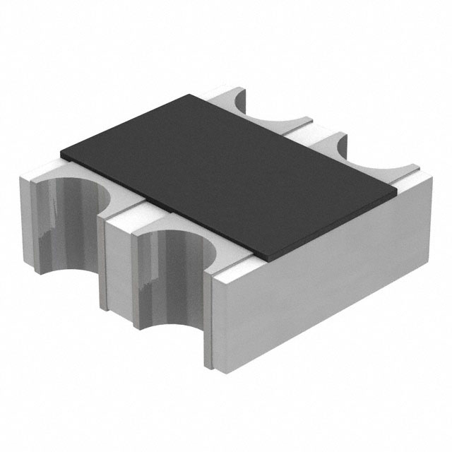 EXB-V4V120JVPanasonic Electronic ComponentsRES ARRAY 2 RES 12 OHM 0606
 -
 EXB-V4V473JVPanasonic Electronic ComponentsRES ARRAY 2 RES 47K OHM 0606
 -
 EXB-V4V823JVPanasonic Electronic ComponentsRES ARRAY 2 RES 82K OHM 0606
 -
 EXB-V4V151JVPanasonic Electronic ComponentsRES ARRAY 2 RES 150 OHM 0606
 -
 EXB-V4V181JVPanasonic Electronic ComponentsRES ARRAY 2 RES 180 OHM 0606
 -
 EXB-V4V331JVPanasonic Electronic ComponentsRES ARRAY 2 RES 330 OHM 0606
 -
 EXB-V4V152JVPanasonic Electronic ComponentsRES ARRAY 2 RES 1.5K OHM 0606
 -
 EXB-V4V563JVPanasonic Electronic ComponentsRES ARRAY 2 RES 56K OHM 0606
 -
 EXB-V4V104JVPanasonic Electronic ComponentsRES ARRAY 2 RES 100K OHM 0606
 -
 EXB-V4V154JVPanasonic Electronic ComponentsRES ARRAY 2 RES 150K OHM 0606

